
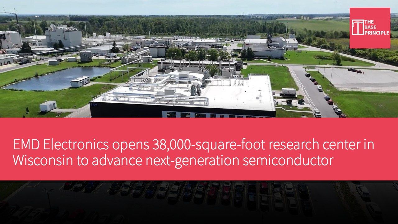
- EMD Electronics opens 38,000-square-foot research center in Wisconsin.
- New center will integrate material synthesis, development and technology transfer.
- EMD will collaborate more closely with customers to address manufacturing needs.
- New facility aims to reduce environmental footprint and achieve LEED certification.
EMD Electronics, the North American electronics business of Germany's Merck KGaA, has opened a 38,000-square-foot research center in Wisconsin with eight laboratories aimed at developing next-generation semiconductor manufacturing materials. The facility is located in Sheboygan Falls and is part of a multi-year, $200 million U.S. investment plan covering semiconductor operations in Wisconsin, California and Oklahoma. Another expansion in Wisconsin is expected to be completed in 2027.
New center integrates multiple functions
The new center integrates material synthesis, development, scale-up and technology transfer in one location. EMD said the setup aims to shorten the process of taking new materials from laboratory development to customer testing and ultimately commercial production.
As manufacturers pack more components into smaller spaces and adopt more complex device designs, advanced chips increasingly rely on specialized materials and chemical processes. EMD supplies the semiconductor industry with products including specialty gases, deposition materials, planarization chemicals and patterning materials. The eight laboratories are dedicated to different stages of the product development cycle, including discovery, development, qualification, analytical development, purification, packaging and hazard testing. Integrating these functions allows researchers to develop materials, determine how to produce them at larger scale, and prepare for production transfer without relying on separate facilities.
EMD said this will also enable it to collaborate more closely with semiconductor customers to address their evolving manufacturing needs.
Environmentally friendly facility design
"The semiconductor industry is entering a period where integrated workflow solutions play a critical role, especially as artificial intelligence drives increasingly complex and demanding performance requirements," said Bing Han, executive vice president of EMD Electronics' Thin Films business. "Materials innovation remains at the core of this transformation, but success increasingly depends on the combination of materials discovery, process expertise and scale-up capabilities."
The Wisconsin Economic Development Corp. is partnering with EMD Electronics on the expansion, and the state agency said it will support technical jobs and strengthen Wisconsin's semiconductor industry influence. The announcement did not specify how many jobs the new facility will create.
The Sheboygan Falls project is part of EMD Electronics' broader effort to expand U.S. semiconductor research and manufacturing capabilities. Its multi-year, $200 million plan also includes recently completed projects in Carlsbad, California, and Catoosa, Oklahoma, as well as a planned Wisconsin expansion in 2027. The spending is part of the company's larger, $1 billion five-year U.S. investment plan announced in 2021 to expand its research and manufacturing operations.
EMD also designed the new Wisconsin laboratories to reduce their environmental footprint. The company said the facility is powered by renewable energy and targets LEED Gold certification, although the certification has not yet been awarded.
For chipmakers, the practical focus of the new center lies in narrowing the gap between finding promising materials and proving they can be reliably manufactured at the scale and quality required for semiconductor production.
Impact of new center on semiconductor industry
EMD Electronics' newly established research center is not only part of its expansion plan but also reflects the semiconductor industry's urgent need for materials innovation. As technology advances, semiconductor manufacturers require more efficient materials development processes to meet increasingly complex product demands. The establishment of this new center will help accelerate the process of materials from laboratory to commercial production, enhance collaboration efficiency with customers, and further strengthen its competitiveness in the market.