
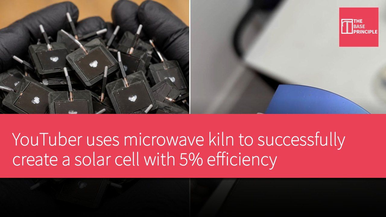
- Dr. Semiconductor created a solar cell with an efficiency of about 5% using a microwave kiln.
- The experiment showcases the potential for producing basic semiconductor devices with readily available equipment in a home workshop.
- The use of a microwave kiln overcomes the limitations of traditional equipment, achieving sufficiently high temperatures for doping.
- Although the output is limited, the project demonstrates the potential for exploring semiconductor processes.
Creating a functional solar cell typically requires specialized equipment to handle silicon, control temperature, and create microscopic electrical structures. However, semiconductor engineer and YouTuber Dr. Semiconductor has showcased a more unconventional method: using a small microwave kiln to transform ordinary silicon wafers into functional photovoltaic cells. The experiment produced a working cell with an efficiency of about 5%, demonstrating that basic semiconductor devices can be manufactured using relatively accessible equipment in a home workshop. While this result does not meet the standards of commercial solar cells, the project offers an intriguing perspective on how to alter the electrical properties of silicon without traditional industrial furnaces.
This further emphasizes Dr. Semiconductor's broader efforts to demonstrate how semiconductor manufacturing techniques can be adapted for home laboratories.
The Key Role of the Microwave Kiln
The key challenge in using a microwave kiln to create solar cells is not only heating the silicon but also forming a junction between two differently doped regions. This junction allows the solar cell to convert incoming light into electrical energy. In this experiment, Dr. Semiconductor started with a p-type silicon wafer, which contains positively charged carriers known as holes. The next step involved introducing phosphorus to the surface of the wafer, creating a thin n-type region. At the intersection of these two regions, a p-n junction is formed, capable of separating the charges generated when light strikes the material.
The phosphorus coating is heated using the small microwave kiln. This kiln utilizes heat-absorbing materials to convert microwave energy into heat, rather than placing the wafer directly in a microwave oven. The temperature achieved in this setup is sufficiently high to allow phosphorus to diffuse into the silicon, a process that typically requires specialized thermal treatment equipment.
Controlling the temperature is crucial. The process requires enough heat to alter the surface of the silicon, but silicon melts at around 1,414°C (2,577°F). The creator's guidance indicates that this specific setup reached approximately 1,000°C (1,832°F), suggesting that relatively simple heating equipment can perform a demanding semiconductor processing step. After cooling the doped wafer, electrical contact points need to be added on both sides. These contact points collect the current generated by the junction when light hits the cell. The creator used soft metals to establish these connections, rather than relying on the specialized contact deposition processes common in semiconductor manufacturing.
The completed device produced a measurable electrical response under illumination, proving that the wafer functions as a photovoltaic cell rather than merely serving as a heating experiment.
Limitations and Challenges of the Experiment
According to the guidance published with the project, the efficiency of the solar cell is about 5%. This is relatively modest compared to commercial silicon solar cells, which typically exceed 20% efficiency. The creator notes that contamination, contact quality, and the lack of an anti-reflective coating are potential areas for improvement. An anti-reflective coating helps reduce the amount of light that reflects away from the cell before it can be absorbed. Better electrical contacts can also enhance the efficiency of current collection. In commercial production, manufacturers carefully control these and other factors to maximize the power generated from a given surface area.
This experiment's significance for home semiconductor manufacturing lies in the fact that the project is not a practical shortcut to producing cheap solar cells. Its output is limited, and its processing methods lack the precision and repeatability required for commercial production. High-temperature equipment and semiconductor processing chemicals also pose significant safety challenges, so this demonstration should not be misconstrued as a simple kitchen project. Its importance lies in showcasing how individuals can explore basic semiconductor processes outside of industrial manufacturing facilities. By combining ordinary silicon wafers, a microwave kiln, and relatively accessible materials, Dr. Semiconductor has demonstrated how to create a functional photovoltaic junction in a home workshop.
This project also highlights the distinction between making a device operational and optimizing it. Producing measurable electrical output is an important first step, but improving efficiency requires better control over materials, processing, surface performance, and electrical contacts.
Exploration and Challenges of Home Semiconductor Manufacturing
This experiment not only demonstrates how to use a microwave kiln for semiconductor manufacturing but also emphasizes the potential for exploring technology in home workshops. While the efficiency of the produced solar cell does not match that of commercial products, its significance lies in breaking the boundaries of traditional manufacturing, allowing more people to access and experiment with semiconductor technology. However, the limitations of this approach cannot be overlooked, as the lack of precision and repeatability makes its commercial application uncertain. Safety issues also pose a barrier to further adoption, highlighting the risks of conducting high-temperature processes in a home environment.