
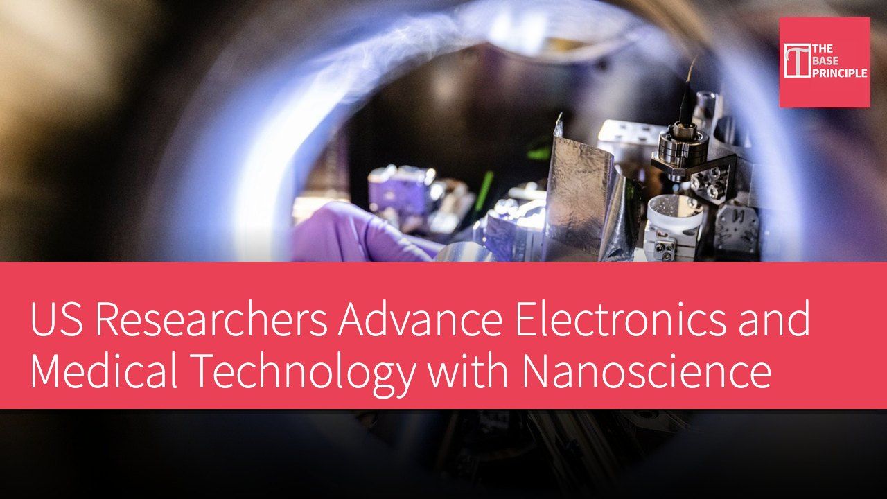
- US researchers are advancing electronics and medical technology using nanoscience.
- At the nanoscale, the properties of matter change dramatically due to quantum effects.
- Argonne's Advanced Photon Source is the world's brightest synchrotron X-ray source.
- The ISN tool enables observation of material behavior and failure processes under real-world conditions.
US researchers are at the forefront of shaping nanoscience, using atomic-level control to accelerate progress in fields such as electronics, energy storage, catalysis, sensing, and medicine. "At Argonne, some of the world's best innovators are transforming nanoscience into next-generation discoveries, pushing ideas that once seemed impossible into the realm of the possible," said Gary Wiederrecht, Director of the Center for Nanoscale Materials and the Nanoscience and Technology division at Argonne.
At the nanoscale, the properties of matter can change dramatically. Modern nanoscience is based on a simple concept: when matter becomes sufficiently small, it behaves differently. At the nanoscale, the properties of matter change dramatically due to quantum effects and forces acting on the material's surface, such as electrostatic forces and other molecular interactions. "What's exciting about nanoscience is that it ultimately concerns the extraordinary changes that occur when materials are shrunk from the macroscopic world to the nanoscale, where almost everything starts to work in different ways," Wiederrecht said.
The Extraordinary Changes of Nanoscience
At the nanoscale, new properties emerge—optical, electrical, chemical—that simply do not exist at larger scales. Scientists and engineers are leveraging these changes to create transformative technologies that were once impossible. Argonne has a strong foundation in materials research, photon science, and advanced instrumentation in the modernization of nanoscience. For decades, its researchers have been dedicated to developing breakthrough tools to redefine how scientists visualize, understand, and engineer matter at the atomic scale.
Argonne's Advanced Photon Source (APS), completed in 1995, is now the world's brightest synchrotron X-ray source. Its comprehensive upgrade, expected to be completed in 2026, will increase the brightness of its X-ray beams by 500 times, allowing researchers to image atomic structures more precisely and track defect formation in materials in real time as they are subjected to different environmental stresses. According to a press release, Argonne's world-class In Situ Nanoprobe (ISN) is a powerful new tool that extends the lab's beamline imaging capabilities into the realm of "in situ" research, where researchers can observe materials as they operate, adapt, and fail under real-world conditions.
Major Upgrade of the Advanced Photon Source
This is a significant step forward for breakthroughs in energy, microelectronics, quantum systems, and advanced manufacturing. "The APS is already one of the world-class engines for understanding matter," said Sarah Wiegold, a physicist at Argonne. "The ISN extends this advantage by adding a particularly important dimension: the ability to probe nanoscale behavior under actual operating conditions." The ISN is linked to complementary technologies at the APS that examine materials at different length scales, timescales, and contrast modes. The combination of these capabilities creates a more complete understanding of complex materials—from the atomic and nanoscale origins of behavior to system-level performance.
The Application Potential of Nanoscience and Technology
The development of nanoscience has profound implications for fields such as electronics and medical technology, as the new properties of matter that emerge at the nanoscale can give rise to entirely new technological applications. The upgrade of Argonne's Advanced Photon Source and its In Situ Nanoprobe will enable researchers to probe and understand material behavior more precisely, which is crucial for breakthroughs in energy, microelectronics, and advanced manufacturing. The combination of these technologies not only enhances the depth of materials research but also provides a broader vision for future innovation.