
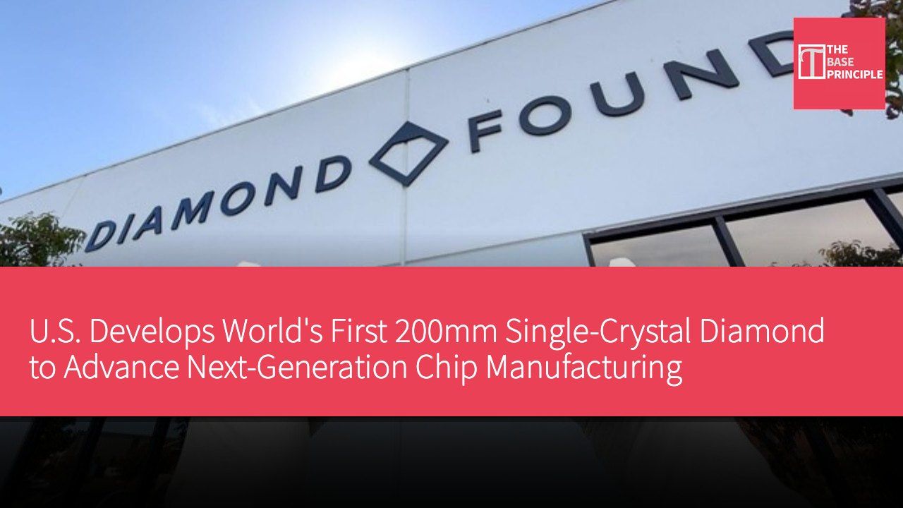
- Diamond Foundry successfully produced the world's first 200mm single-crystal diamond, advancing semiconductor manufacturing.
- Single-crystal diamonds possess excellent thermal conductivity, effectively dissipating heat from high-performance processors.
- Producing large single-crystal diamonds presents significant engineering challenges, but the CVD method offers a new pathway.
- The company plans to expand manufacturing in Spain, aiming to transform single-crystal diamonds into industrial semiconductor materials.
Diamond Foundry announced that it has successfully produced the world's first 200mm (7.9 inches) single-crystal diamond, a development that could bring one of nature's most thermally conductive materials closer to semiconductor manufacturing. The San Francisco-based company revealed this milestone on November 6, describing it as the result of 25 years of effort to grow large continuous diamond crystals. This achievement is significant because diamonds possess a range of properties that can address some challenges faced by advanced electronic products, particularly in effectively removing heat generated by high-performance processors.
However, the new crystal currently showcased by the company remains in an unpolished growth state. This 200mm crystal is a continuous structure, rather than being composed of multiple small diamonds or containing multiple grains like polycrystalline wafers. This distinction is crucial, as grain boundaries and defects can affect the efficiency of heat and charge conduction within the material.
Challenges in Growing Single-Crystal Diamonds
The difficulty in growing single-crystal diamonds lies in the tightly ordered lattice arrangement of carbon atoms that make up the diamond. Producing large single-crystal structures requires maintaining this atomic arrangement throughout the growth process, as even minor inconsistencies can introduce defects that undermine the desired properties. Traditional high-pressure, high-temperature methods can produce synthetic diamonds, but scaling this up to single crystals of semiconductor size presents significant engineering challenges. Chemical vapor deposition (CVD) offers an alternative pathway, growing diamonds from carbon-containing gases in a controlled environment. Microwave plasma CVD is particularly important in the research of large, high-quality diamond crystals.
Diamond Foundry's previous milestones provide some context. The company had previously announced the production of a 100mm (3.9 inches) single-crystal diamond wafer, utilizing diamond heteroepitaxy technology, which grows crystals on different substrates and promotes the adoption of an ordered diamond lattice. The company has not disclosed whether the newly announced 200mm crystal used the same process.
According to CEO Martin Roscheisen, the latest achievement required advancements in plasma physics, reactor engineering, growth chemistry, crystal engineering, and manufacturing control. He also praised Stefan Gsell and Martin Fischer, who began research on the scaling of single-crystal diamonds 25 years ago.
The Potential of Diamonds in Electronic Products
One reason diamonds are garnering attention in the semiconductor industry is their excellent thermal conductivity. High-purity single-crystal diamonds have a thermal conductivity of about 2,000 watts per meter per Kelvin (W/m·K) at room temperature, several times that of copper. This property could make diamonds useful for thermal management in increasingly powerful electronic devices. Modern artificial intelligence processors and high-performance computing systems concentrate large amounts of electrical power in relatively small areas. Localized heat buildup can limit operational performance, increase cooling demands, and accelerate component degradation. Diamonds could serve as thermal spreaders or substrates in advanced chip packaging, helping to divert heat away from hotspots.
Its bandgap of approximately 5.47 electron volts also makes it a candidate material for high-power and high-frequency electronic products that must operate under demanding electrical conditions.
However, diamonds cannot simply replace silicon. Manufacturing electronic devices from diamonds remains challenging, particularly because reliably controlling their electrical properties through doping is difficult. Integrating diamonds with existing semiconductor materials and manufacturing processes also requires further development.
The distinction between growing large crystals and producing usable semiconductor wafers is crucial. The first 200mm sample showcased by Diamond Foundry is an unpolished direct growth product. It requires further processing and characterization to determine its suitability for chip manufacturing. Manufacturers must achieve consistent thickness, surface flatness, low defect density, and reliable electrical and thermal properties within the usable wafer area. They must also demonstrate reproducibility across multiple production runs and ensure that the material can be integrated into device manufacturing. Diamond Foundry stated that the achievement of 200mm makes the prospect of future 300mm (11.8 inches) crystals feasible, but it has not provided a timeline or detailed manufacturing data for this next step.
Future Plans for Manufacturing Expansion
The company also plans to expand its manufacturing ambitions in Spain through a $2.77 billion project supported by the European Chips Act. Its broader goal is to transform single-crystal diamonds into an industrial semiconductor material, rather than being limited to providing specialty products in limited sizes.
Item Specification Crystal Diameter 200 mm Thermal Conductivity Approximately 2,000 W/m·K Bandgap Approximately 5.47 eV
The Impact of Single-Crystal Diamonds on the Semiconductor Industry
The successful production of single-crystal diamonds marks an important milestone for the semiconductor industry, as their thermal conductivity surpasses that of traditional materials, effectively addressing thermal management issues in electronic devices. With the increasing demand for high-performance processors, materials capable of effective heat dissipation are becoming increasingly important. Although diamonds still face challenges in production and electrical property control, their potential has generated optimism for future developments. Diamond Foundry's expansion plans demonstrate ambition to transform single-crystal diamonds into industrial semiconductor materials, which could change the manufacturing processes of future electronic products.