
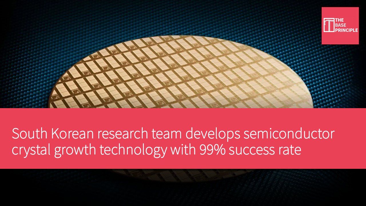
- Technology developed by South Korean researchers can control crystal formation with a success rate exceeding 99%.
- The method solves a major obstacle in stacked chip manufacturing, ensuring precise formation of semiconductor layers.
- Researchers use an oxide barrier to release oxygen to control the starting position of crystal growth.
- The properties of two-dimensional semiconductors make them a research focus for future chip materials.
South Korean researchers have developed a semiconductor manufacturing technology that can control the formation of single crystals in 400 patterned growth areas with a success rate exceeding 99%, a technique that could help manufacturers build vertically stacked computing chips. The technology allows researchers to grow single molybdenum disulfide (MoS₂) crystals at predetermined locations — a semiconductor just a few atomic layers thick — rather than letting multiple crystals form randomly. A team led by the Korea Advanced Institute of Science and Technology (KAIST), in collaboration with UNIST, Hanyang University, and TDS Innovation, developed the method, which uses oxygen released from an oxide barrier to control the starting position of crystal growth.
Overcoming obstacles in stacked chips
The researchers said the method can solve a major obstacle in manufacturing stacked chips: semiconductor layers must form precisely atop existing circuitry to avoid introducing defects that affect performance.
Oxygen controls crystal formation. Conventional semiconductor growth methods can define the general area where a film forms, but controlling the exact starting point of each crystal remains difficult. When several crystals grow independently and meet, they form grain boundaries. These boundaries disrupt the regular arrangement of atoms and can interfere with the movement of electrons in the semiconductor. The researchers developed a process called etch-flux-mediated single-center nucleation (EF-SCN). Nucleation is the initial stage of crystal formation, when atoms begin arranging into an ordered structure. The process uses an oxide barrier, such as hafnium oxide (HfO₂), surrounding the designated growth area.
Oxygen released from the barrier acts as an etchant, suppressing unwanted crystal formation. The oxygen's influence is strongest at the edges of the patterned area and gradually weakens toward the center. This creates conditions favorable for a crystal to form at a single central point. Once growth begins there, the process also suppresses the formation of additional crystals nearby.
The future of two-dimensional semiconductors
Using this method, the researchers successfully grew single MoS₂ crystals at the designated central positions in more than 99% of the 400 patterns. The team also demonstrated selective metal deposition using structures combining molybdenum disulfide and molybdenum diselenide (MoSe₂). In these structures, a thin platinum metal film formed selectively on the MoSe₂ regions, showing another way to control material placement during semiconductor manufacturing.
Stacked chips draw closer. Because two-dimensional semiconductors retain their semiconducting properties even when just a few atomic layers thick, they are being studied as materials for future chips. Their small thickness could allow manufacturers to vertically stack compute and memory elements, reducing the distance data must travel between them. Moving data within a chip consumes energy and causes processing delays; placing components closer together can lower these costs, especially in systems handling large computational workloads. However, producing such chips requires precise control over semiconductor growth on surfaces that contain previously fabricated circuitry.
KAIST's technology offers a possible way to directly grow high-quality two-dimensional materials at designated locations, avoiding the need to fabricate them separately and transfer them onto the wafer.
The researchers examined the mechanism through growth experiments and simulations, but have not yet demonstrated a complete stacked processor or measured improvements in computing speed or energy consumption. The study establishes control over crystal nucleation, not commercial chip performance. Further development is needed to determine whether the method can be integrated into semiconductor manufacturing at scale. The research was published on October 8 in the journal Nature.
Potential impact of the new technology on semiconductor manufacturing
The development of this technology is significant for the semiconductor industry because it effectively solves the precise control problem in stacked chip manufacturing. With the rise of two-dimensional semiconductor materials, this technology can not only improve production efficiency but also promote the creation of more miniaturized and high-performance computing elements. This is crucial for growing future computing demands and reducing energy consumption. However, commercial application of the technology still requires further validation and improvement, which will determine its actual value in the market.